The Central Processing Unit (CPU): Its Components And Functionality
Image by Michael Schwarzenberger from Pixabay
An Introduction To The CPU, What It Does, How It Works, And How It Came To Be
The legacies of earlier designs, such as Babbage’s difference engine and the mainframe punch card systems of the 1970s, have a significant impact on today’s computer systems. In the first article in this historical series, Computer history and modern computers for sysadmins, I discussed several precursors to the modern computer and listed characteristics that define what we call a computer today.
In this article, I discuss the central processing unit (CPU), including its components and functionality. Many of the topics refer back to the first article, so be sure to read it if you haven’t already.
The central processing unit (CPU)
The CPU in modern computers is the embodiment of the “mill” in Babbage’s difference engine. The term central processing unit originated way back in the mists of computer time when a single massive cabinet contained the circuitry required to interpret machine level program instructions and perform operations on the data supplied. The central processing unit also completed all processing for any attached peripheral devices. Peripherals included printers, card readers, and early storage devices such as drum and disk drives. Modern peripheral devices have a significant amount of processing power themselves and off-load some processing tasks from the CPU. This frees the CPU up from input/output tasks so that its power is applied to the primary task at hand.
Early computers only had one CPU and could only perform one task at a time.
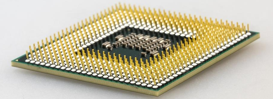
We retain the term CPU today, but now it refers to the processor package on a typical motherboard. Figure 1 displays a standard Intel processor package.

There is really nothing to see here other than the processor package itself. The processor package is a chip containing the processor(s) sealed inside a metal container and mounted on a small printed circuit (PC) board. The package is simply dropped into place in the CPU socket on a motherboard and secured with a locking lever arrangement. A CPU cooler attaches to the processor package. There are several different physical sockets with specific numbers of contacts, so getting the correct package to fit the motherboard socket is essential if you build your own computers.
How the CPU works
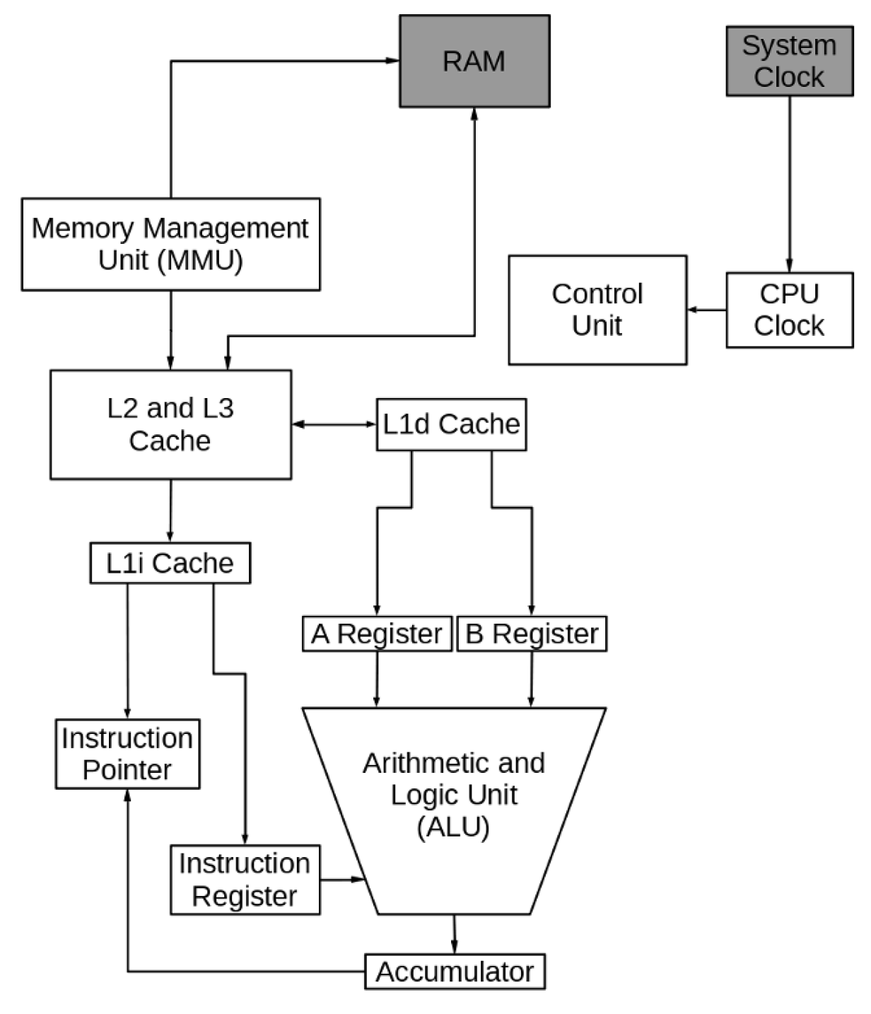
Let’s look at the CPU in more detail. Figure 2 is a conceptual diagram of a hypothetical CPU so that you can visualize the components more easily. The RAM and system clock are shaded because they are not part of the CPU and are only shown for clarity. Also, no connections between the CPU clock and the control unit to the CPU components are drawn in. Suffice it to say that signals from the clock and the control unit are an integral part of every other component.

This design does not look particularly simple, but the reality is even more complicated. This figure is sufficient for our purposes without being overly complex.
Arithmetic logic unit
The arithmetic logic unit (ALU) performs the arithmetic and logical functions that are the work of the computer. The A and B registers hold the input data, and the accumulator receives the result of the operation. The instruction register contains the instruction that the ALU is to perform.
For example, when adding two numbers, one number is placed in the A register and the other in the B register. The ALU performs the addition and puts the result in the accumulator. If the operation is a logical one, the data to be compared is placed into the input registers. The result of the comparison, a 1 or 0, is put in the accumulator. Whether this is a logical or arithmetic operation, the accumulator content is then placed into the cache location reserved by the program for the result.
There is another type of operation performed by the ALU. The result is an address in memory, and it is used to calculate a new location in memory to begin loading instructions. The result is placed into the instruction pointer register.
Instruction register and pointer
The instruction pointer specifies the location in memory containing the next instruction to be executed by the CPU. When the CPU completes the execution of the current instruction, the next instruction is loaded into the instruction register from the memory location pointed to by the instruction pointer.
After the instruction is loaded into the instruction register, the instruction register pointer is incremented by one instruction address. Incrementing allows it to be ready to move the next instruction into the instruction register.
Cache
The CPU never directly accesses RAM. Modern CPUs have one or more layers of cache. The CPU’s ability to perform calculations is much faster than the RAM’s ability to feed data to the CPU. The reasons for this are beyond the scope of this article, but I will explore it further in the next article.
Cache memory is faster than the system RAM, and it is closer to the CPU because it is on the processor chip. The cache provides data storage and instructions to prevent the CPU from waiting for data to be retrieved from RAM. When the CPU needs data—and program instructions are also considered to be data—the cache determines whether the data is already in residence and provides it to the CPU.
If the requested data is not in the cache, it’s retrieved from RAM and uses predictive algorithms to move more data from RAM into the cache. The cache controller analyzes the requested data and tries to predict what additional data will be needed from RAM. It loads the anticipated data into the cache. By keeping some data closer to the CPU in a cache that is faster than RAM, the CPU can remain busy and not waste cycles waiting for data.
Our simple CPU has three levels of cache. Levels 2 and 3 are designed to predict what data and program instructions will be needed next, move that data from RAM, and move it ever closer to the CPU to be ready when needed. These cache sizes typically range from 1 MB to 32 MB, depending upon the speed and intended use of the processor.
The Level 1 cache is closest to the CPU. In our CPU, there are two types of L1 cache. L1i is the instruction cache, and L1d is the data cache. Level 1 cache sizes typically range from 64 KB to 512 KB.
Memory management unit
The memory management unit (MMU) manages the data flow between the main memory (RAM) and the CPU. It also provides memory protection required in multitasking environments and conversion between virtual memory addresses and physical addresses.
CPU clock and control unit
All of the CPU components must be synchronized to work together smoothly. The control unit performs this function at a rate determined by the clock speed and is responsible for directing the operations of the other units by using timing signals that extend throughout the CPU.
Random access memory (RAM)
Although the RAM, or main storage, is shown in this diagram and the next, it is not truly a part of the CPU. Its function is to store programs and data so that they are ready for use when the CPU needs them.
How it works
CPUs work on a cycle that is managed by the control unit and synchronized by the CPU clock. This cycle is called the CPU instruction cycle, and it consists of a series of fetch/decode/execute components. The instruction, which may contain static data or pointers to variable data, is fetched and placed into the instruction register. The instruction is decoded, and any data is placed into the A and B data registers. The instruction is executed using the A and B registers, with the result put into the accumulator. The CPU then increases the instruction pointer’s value by the length of the previous one and begins again.
The basic CPU instruction cycle looks like this.

The need for speed
Although the basic CPU works well, CPUs that run on this simple cycle can be used even more efficiently. There are multiple strategies for boosting CPU performance, and we look at two of them here.
Supercharging the instruction cycle
One problem early CPU designers encountered was wasted time in the various CPU components. One of the first strategies for improving CPU performance was overlapping the portions of the CPU instruction cycle to utilize the various parts of the CPU more fully.
For example, when the current instruction has been decoded, the next one is fetched and placed into the instruction register. As soon as that has occurred, the instruction pointer is updated with the next instruction’s memory address. The use of overlapping instruction cycles is illustrated in Figure 4.

This design looks nice and smooth, but factors such as waiting for I/O can disrupt the flow. Not having the proper data or instructions in the cache requires the MMU to locate the correct ones and move them to the CPU, and that can take some time. Certain instructions also take more CPU cycles to complete than others, interfering with smooth overlapping.
Nevertheless, this is a powerful strategy for improving CPU performance.
Hyperthreading
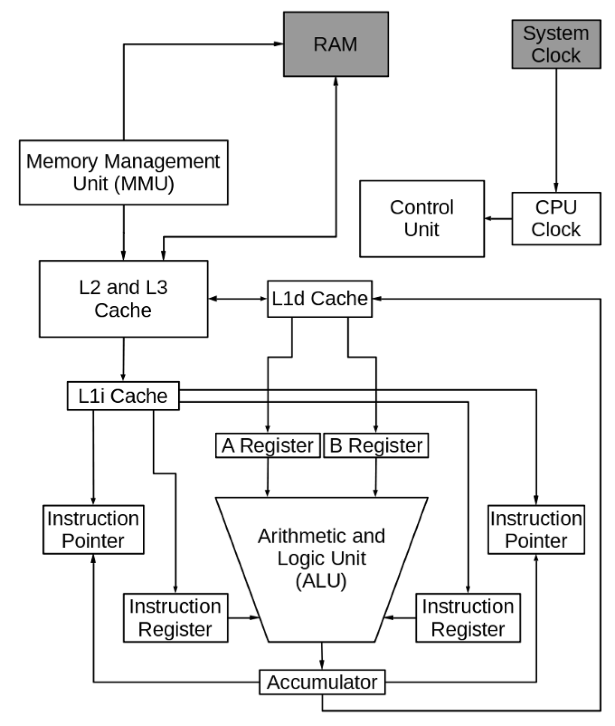
Another strategy to improve CPU performance is hyperthreading. Hyperthreading makes a single processor core work like two CPUs by providing two data and instruction streams. Adding a second instruction pointer and instruction register to our hypothetical CPU, as shown in Figure 5, causes it to function like two CPUs, executing two separate instruction streams during each instruction cycle. Also, when one execution stream stalls while waiting for data—again, instructions are also data—the second execution stream continues processing. Each core that implements hyperthreading is the equivalent of two CPUs in its ability to process instructions.

Remember that this is a very simplified diagram and explanation of our hypothetical CPU. The reality is far more complex.
More terminology
I have encountered a lot of different CPU terminology. To define the terminology a little more explicitly, let’s look at the CPU itself by using the lscpu command.
[root@hornet ~]# lscpu
Architecture:                    x86_64
CPU op-mode(s):                  32-bit, 64-bit
Byte Order:                      Little Endian
Address sizes:                   39 bits physical, 48 bits virtual
CPU(s):                          12
On-line CPU(s) list:             0-11
Thread(s) per core:              2
Core(s) per socket:              6
Socket(s):                       1
NUMA node(s):                    1
Vendor ID:                       GenuineIntel
CPU family:                      6
Model:                           158
Model name:                      Intel(R) Core(TM) i7-8700 CPU @ 3.20GHz
Stepping:                        10
CPU MHz:                         4300.003
CPU max MHz:                     4600.0000
CPU min MHz:                     800.0000
BogoMIPS:                        6399.96
Virtualization:                  VT-x
L1d cache:                       192 KiB
L1i cache:                       192 KiB
L2 cache:                        1.5 MiB
L3 cache:                        12 MiB
NUMA node0 CPU(s):               0-11
<SNIP>
The Intel processor shown above is a package that plugs into a single socket on the motherboard. The processor package contains six cores. Each core is capable of hyperthreading, so each can run two simultaneous threads for a total of 12 CPUs.
My definitions:
- Core – A core is the smallest physical hardware unit capable of performing the task of processing. It contains one ALU and one or two sets of supporting registers. The second set of registers and supporting circuitry enables hyperthreading. One or more cores can be combined into a single physical package.
- CPU – A logical hardware unit capable of processing a single thread of execution. The modern use of the term central processing unit refers to the total number of threads that a processor package is capable of executing simultaneously. A single-core processor that does not support hyperthreading is the equivalent of a single CPU. In this case, CPU and core are synonymous. A hyperthreading processor with a single core is the functional equivalent of two CPUs. A hyperthreading processor with eight cores is the functional equivalent of 16 CPUs.
- Package – The physical component that contains one or more cores, such as that shown in Figure 1 above.
- Processor – 1) A device that processes program instructions to manipulate data. 2) Frequently used as a synonym for package.
- Socket – Sometimes used as another synonym for package, but it more accurately refers to the physical socket on the motherboard into which the processor package is inserted.
The terms socket, processor, and package are often used interchangeably, which can cause some confusion. As we see from the lscpu command results above, Intel provides us with its own terminology, and I consider that the authoritative source. In reality, we all use those terms in various ways, but as long as we understand each other at any given point, that is what really matters.
Notice that the processor above has two Level 1 caches of 512 KiB each, one for instructions (L1i) and one for data (L1d). The Level 1 cache is closest to the CPU, and it speeds things up to have instructions and data separate at this point. Level 2 and Level 3 caches are larger, but instructions and data co-exist in each.
What does this all mean?
Good question. Back in the early days of mainframes, each computer had only a single CPU and was incapable of running more than one program simultaneously. The mainframe might run payroll, then inventory accounting, then customer billing, and so on, but only one application could run at a time. Each program had to finish before the system operator could start the next.
Some early attempts at running multiple programs at once took a simple approach and were aimed at better utilization of a single CPU. For example, program1 and program2 were loaded, and program1 ran until it was blocked waiting for I/O to occur. At that point, program2 ran until it was blocked. This approach was called multi-processing and helped to fully utilize valuable computer time.
Early attempts at multitasking all involved switching the execution context of a single CPU very rapidly between the execution streams of multiple tasks. This practice is not true multitasking as we understand it because, in reality, only a single thread of execution is processed at a time. It is more correctly called time-sharing.
Modern computers, from smart watches and tablets to supercomputers, all support true multitasking with multiple CPUs. Multiple CPUs enable computers to run many tasks simultaneously. Each CPU performs its own functions at the same time as all the other CPUs. An eight-core processor with hyperthreading (i.e., 16 CPUs) can run 16 tasks simultaneously.
Final thoughts
We looked at a conceptualized and simplified CPU to learn a bit about structures. I barely skimmed the surface of processor functionality in this article. You can learn more by taking the embedded links for the topics we explored.
Remember that the diagrams and descriptions in this article are purely conceptual and do not represent any actual CPU.
In the next article of this series, I’ll look at RAM and disk drives as different types of storage and why each is necessary to modern computers.